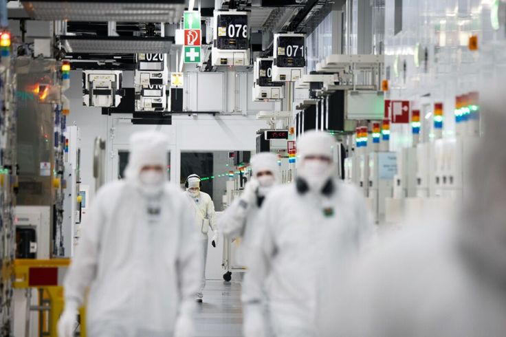
Semiconductor cleanrooms are highly controlled environments designed to support the manufacturing of semiconductors — the delicate, essential components found in virtually every electronic device. From smartphones to satellites, semiconductor chips are critical, and their production demands absolute precision and minimal contamination.
In this article, we’ll explore what semiconductor cleanrooms are, why they’re necessary, how they’re classified, and how they’re designed to meet the stringent standards of modern chip fabrication.
What Are Semiconductors and Why Do They Require Cleanrooms?
Semiconductors are materials, typically made from purified silicon, that have electrical conductivity between conductors (like metals) and insulators (like ceramics). Their unique properties allow them to control electrical current, making them foundational to transistors, microprocessors, and memory devices.
To manufacture semiconductors, silicon is melted, shaped into cylindrical ingots, sliced into ultra-thin wafers, and layered through complex chemical processes. These operations require extreme cleanliness. A single microscopic particle can damage an entire wafer and ruin thousands of microchips.
That’s where semiconductor cleanrooms come in — providing particle-controlled environments that meet ISO or Federal Standard classifications, enabling precise, consistent chip fabrication.
Why Semiconductor Cleanrooms Are So Important
Unlike cleanrooms used in industries like food processing or pharmaceuticals, semiconductor cleanrooms are among the most demanding. That’s because the components being made are nanoscale in size — one speck of dust can cause an entire batch to fail.
Modern semiconductors feature line widths below 10 nanometers, which requires cleanroom environments with:
Extremely low airborne particle levels
Precise control of temperature and humidity
Protection against electrostatic discharge
Advanced air filtration and pressure differentials
Applications of Semiconductor Cleanrooms
Semiconductors are used in a wide range of industries. Cleanrooms enable their production in the following fields:
Computing (laptops, servers, cloud infrastructure)
Mobile Devices (smartphones, tablets)
Automotive Manufacturing (electric vehicles, ADAS systems)
Aerospace & Defense (navigation, guidance systems)
Consumer Electronics (home appliances, IoT devices)
Robotics & Automation
Medical Devices (implantable electronics, diagnostics)
Semiconductor Cleanroom Classifications
Semiconductor cleanrooms are generally classified using the ISO 14644-1 standard, which defines cleanroom classes based on the number of particles ≥0.5 μm per cubic meter of air.
| ISO Class | Max. Particles ≥0.5μm / m³ | FED STD 209E Equivalent | Typical Use |
|---|---|---|---|
| ISO 4 | 10,000 | Class 10 | Photolithography |
| ISO 5 | 100,000 | Class 100 | Etching, deposition |
| ISO 6 | 1,000,000 | Class 1,000 | Packaging, assembly |
| ISO 7-8 | Looser controls | Class 10,000+ | Testing & storage |
Key Design Features of Semiconductor Cleanrooms
Designing a semiconductor cleanroom requires precision engineering. Common features include:
1. Advanced Filtration Systems
Most cleanrooms use ULPA filters (99.9995% efficiency for 0.12 µm particles), which are more effective than standard HEPA filters (99.97% at 0.3 µm).
2. Controlled Airflow
Unidirectional (laminar) airflow ensures particles are swept away from critical zones. Raised flooring is often used to support bottom-up air return systems.
3. Static Dissipation
Electrostatic discharge (ESD) can destroy semiconductor components. Cleanrooms use static-dissipative flooring, furniture, and garments to neutralize risk.
4. Temperature & Humidity Control
Typical specs:
Temperature: ±1°F (around 21°C)
Relative Humidity: 35%–60%
Variations can alter chemical behaviors or damage wafers.
5. Material Compatibility
Construction materials must resist outgassing and particle shedding. Common choices include:
Stainless steel
PVC wall panels
HDPE surfaces
Common Semiconductor Cleanroom Challenges
Cost: High initial and operational costs due to energy usage and maintenance
Training: Workers must follow strict gowning and hygiene protocols
Validation: Cleanrooms must undergo frequent validation to remain compliant
Summary: Why Semiconductor Cleanrooms Matter
Semiconductor cleanrooms are a cornerstone of modern electronics manufacturing. Their role in producing ultra-precise, contamination-free chips makes them essential to national security, global communication, and future innovation.
As chip complexity increases and line widths shrink, the demand for advanced cleanroom design, monitoring, and compliance will continue to grow.
External Resources
FAQ – Semiconductor Cleanrooms
Q1: What is the most common cleanroom class for semiconductor fabrication?
ISO 4 and ISO 5 (Class 10 and Class 100) are commonly used in photolithography and wafer processing.
Q2: Why is static control important in cleanrooms?
Electrostatic discharge can damage sensitive chips. Static-dissipative materials prevent charge buildup.
Q3: Can cleanroom operations be automated?
Yes. Many facilities integrate robotics to minimize human contamination and ensure safety in hazardous processes.
Q4: What materials are used in constructing semiconductor cleanrooms?
Stainless steel, vinyl, PVC panels, and other low-shedding, non-reactive materials.